Theoretical Paper
- Computer Organization
- Data Structure
- Digital Electronics
- Object Oriented Programming
- Discrete Mathematics
- Graph Theory
- Operating Systems
- Software Engineering
- Computer Graphics
- Database Management System
- Operation Research
- Computer Networking
- Image Processing
- Internet Technologies
- Micro Processor
- E-Commerce & ERP
Practical Paper
Industrial Training

Logic Gates
There are digital circuits which either allow a signal to pass through or stop it. The circuits other wise called as gate allows the signal to pass only when some logical condition are satisfied. Under such condition the circuits are called logic gates. They are building blocks of any digital system. The basic logic gates are:
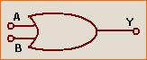
1. OR gate
2. AND gate and
3. NOT gate
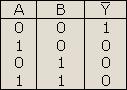
Truth table is a table that shows all possible input combination and the corresponding output combination for a logic gate.
The Boolean algebra '+' or addition symbol is referred to as OR operation.
i.e. A + B (Read A or B)
The symbol '.' or multiplication symbol is referred to as AND operation.
i.e. A.B (Read A AND B)
The symbol (-) above the input i.e.
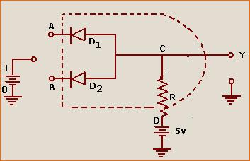
Realisation of an OR gate using diodes
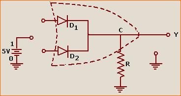
1. When both A and B are earthed (i.e. connected to low input 0), both the diodes do not conduct and no voltage develops across R. Therefore the voltage at C is zero with respect to earth. Hence the output Y is 0 (in levels).
2. When A = 0 and B = 1 (i.e., connected to positive terminal), the diode D2 conducts but D1 does not. Since D2 is ideal, no voltage drop takes place across D2 and a full voltage drop of 5V takes place across R at C, +5V with respect to earth. Therefore Y is 1 (in level).
3. When A = 1 and B = 0, D1 conducts but D2 does not. For the same reason as stated above the output Y is 1 (in level).
4. When A = 1 and B = 1, both diodes conducts since the diodes are ideal and connected in parallel, the voltage drop across R cannot exceed 5V, with C at +5V with respect to earth. Hence the output Y will be 1 (in level).
The truth table of OR gate
| A | B | C |
| 0 | 0 | 0 |
| 0 | 1 | 1 |
| 1 | 0 | 1 |
| 1 | 1 | 1 |
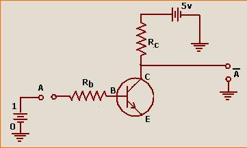
The AND gate
1. When A = 0 and B = 0 both diode D1 and D2 get forward biased and hence conduct. The diodes being ideal, no voltage drop takes place across either diode. Therefore potential difference of 5V takes place across R, with C at zero potential with respect to earth. Thus the output Y is 0 (in level).
2. When A = 0, B = 1, D1 conducts diode D2 will not. Since D1 is ideal, no voltage drop occurs it. Therefore a voltage drop of 5V takes place across R, having D at +5V and C at zero with respect to earth. The output is 0 (in levels).
3. When A = 1, B = 0 for same reason, output is 0.
When A = 1, B = 1 none of diodes conduct and so no current flows through R. The potential at C is equal to potential at D which is +5V with respect to earth. Hence output Y is 1.
| A | B | Y |
| 0 | 0 | 0 |
| 0 | 1 | 0 |
| 1 | 0 | 0 |
| 1 | 1 | 1 |
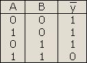
The NOT gate
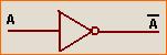
(i) When A = 0, the base of transistor also get earthed. Now emitter base function is not forward biased but base-collector function is reverse biased. As the emitter current is zero, the base current is also zero and hence the collector current will also be zero. Hence the output Y is 1 (in level).
(ii) When A = 1, the emitter base function gets forward biased. There will be emitter current, base current and collector current. The value of Rb and Rc can be adjusted so that large Ic can flow. The potential difference across Rc due to forward biasing of emitter is just 5V equal and opposite to the potential difference across Rc due to battery in collector circuit. Therefore the output is 0 (in level).

NOT gate is realised by transistor when A input is zero (grounded) so base is grounded.
All the voltage drops across collector and emitter, so we will get high output.
When A is given +5 voltage Base current increases consequentially collector current increases in common emitter configuration. Therefore voltage drop across Rc increase but voltage drop collects and emitter is zero, so output is zero.
Even giving high input at A out put is zero.
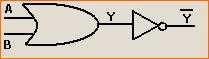
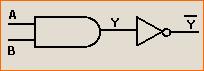
NAND Gate
NOR gate