Theoretical Paper
- Computer Organization
- Data Structure
- Digital Electronics
- Object Oriented Programming
- Discrete Mathematics
- Graph Theory
- Operating Systems
- Software Engineering
- Computer Graphics
- Database Management System
- Operation Research
- Computer Networking
- Image Processing
- Internet Technologies
- Micro Processor
- E-Commerce & ERP
Practical Paper
Industrial Training

Sequential Logic Circuits
Sequential Logic Basics
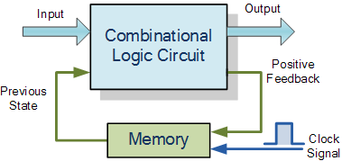
Unlike Combinational Logic circuits that change state depending upon the actual signals being applied to their inputs at that time, Sequential Logic circuits have some form of inherent “Memory” built in to them as they are able to take into account their previous input state as well as those actually present, a sort of ”before” and “after” effect is involved with sequential logic circuits.
In other words, the output state of a “sequential logic circuit” is a function of the following three states, the “present input”, the “past input” and/or the “past output”. Sequential Logic circuits remember these conditions and stay fixed in their current state until the next clock signal changes one of the states, giving sequential logic circuits “Memory”.
Sequential logic circuits are generally termed as two state or Bistable devices which can have their output or outputs set in one of two basic states, a logic level “1” or a logic level “0” and will remain “latched” (hence the name latch) indefinitely in this current state or condition until some other input trigger pulse or signal is applied which will cause the bistable to change its state once again.
Sequential Logic Representation
The word “Sequential” means that things happen in a “sequence”, one after another and in Sequential Logic circuits, the actual clock signal determines when things will happen next. Simple sequential logic circuits can be constructed from standard Bistable circuits such as: Flip-flops, Latches and Counters and which themselves can be made by simply connecting together universal NAND Gates and/or NOR Gates in a particular combinational way to produce the required sequential circuit.
Classification of Sequential Logic
As standard logic gates are the building blocks of combinational circuits, bistable latches and flip-flops are the basic building blocks of Sequential Logic Circuits. Sequential logic circuits can be constructed to produce either simple edge-triggered flip-flops or more complex sequential circuits such as storage registers, shift registers, memory devices or counters. Either way sequential logic circuits can be divided into the following three main categories:
1. Event Driven – asynchronous circuits that change state immediately when enabled.
2. Clock Driven – synchronous circuits that are synchronised to a specific clock signal.
3. Pulse Driven – which is a combination of the two that responds to triggering pulses.
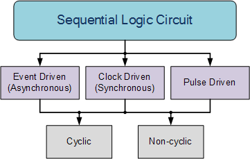
As well as the two logic states mentioned above logic level “1” and logic level “0”, a third element is introduced that separates sequential logic circuits from their combinational logic counterparts, namely TIME. Sequential logic circuits return back to their original steady state once reset and sequential circuits with loops or feedback paths are said to be “cyclic” in nature.
We now know that in sequential circuits changes occur only on the application of a clock signal making it synchronous, otherwise the circuit is asynchronous and depends upon an external input. To retain their current state, sequential circuits rely on feedback and this occurs when a fraction of the output is fed back to the input and this is demonstrated as:
Sequential Feedback Loop
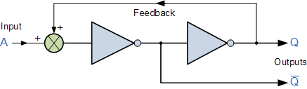
The two inverters or NOT gates are connected in series with the output at Q fed back to the input. Unfortunately, this configuration never changes state because the output will always be the same, either a “1” or a “0”, it is permanently set. However, we can see how feedback works by examining the most basic sequential logic components, called the SR flip-flop.
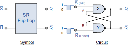
SR Flip-Flop
The SR flip-flop, also known as a SR Latch, can be considered as one of the most basic sequential logic circuit possible. This simple flip-flop is basically a one-bit memory bistable device that has two inputs, one which will “SET” the device (meaning the output = “1”), and is labelled S and another which will “RESET” the device (meaning the output = “0”), labelled R.
Then the SR description stands for “Set-Reset”. The reset input resets the flip-flop back to its original state with an output Q that will be either at a logic level “1” or logic “0” depending upon this set/reset condition.
A basic NAND gate SR flip-flop circuit provides feedback from both of its outputs back to its opposing inputs and is commonly used in memory circuits to store a single data bit. Then the SR flip-flop actually has three inputs, Set, Reset and its current output Q relating to it’s current state or history. The term “Flip-flop” relates to the actual operation of the device, as it can be “flipped” into one logic Set state or “flopped” back into the opposing logic Reset state.
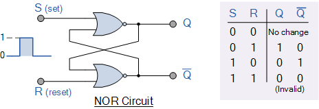
The NAND Gate SR Flip-Flop
The simplest way to make any basic single bit set-reset SR flip-flop is to connect together a pair of cross-coupled 2-input NAND gates as shown, to form a Set-Reset Bistable also known as an active LOW SR NAND Gate Latch, so that there is feedback from each output to one of the other NAND gate inputs. This device consists of two inputs, one called the Set, S and the other called the Reset, R with two corresponding outputs Q and its inverse or complement Q (not-Q) as shown below.
The Basic SR Flip-flop
The Set State
Consider the circuit shown above. If the input R is at logic level “0” (R = 0) and input S is at logic level “1” (S = 1), the NAND gate Y has at least one of its inputs at logic “0” therefore, its output Q must be at a logic level “1” (NAND Gate principles). Output Q is also fed back to input “A” and so both inputs to NAND gate X are at logic level “1”, and therefore its output Q must be at logic level “0”.
Again NAND gate principals. If the reset input R changes state, and goes HIGH to logic “1” with S remaining HIGH also at logic level “1”, NAND gate Y inputs are now R = “1” and B = “0”. Since one of its inputs is still at logic level “0” the output at Q still remains HIGH at logic level “1” and there is no change of state. Therefore, the flip-flop circuit is said to be “Latched” or “Set” with Q = “1” and Q = “0”.
Reset State
In this second stable state, Q is at logic level “0”, (not Q = “0”) its inverse output at Q is at logic level “1”, (Q = “1”), and is given by R = “1” and S = “0”. As gate X has one of its inputs at logic “0” its output Q must equal logic level “1” (again NAND gate principles). Output Q is fed back to input “B”, so both inputs to NAND gate Y are at logic “1”, therefore, Q = “0”.
If the set input, S now changes state to logic “1” with input R remaining at logic “1”, output Q still remains LOW at logic level “0” and there is no change of state. Therefore, the flip-flop circuits “Reset” state has also been latched and we can define this “set/reset” action in the following truth table.
Truth Table for this Set-Reset Function
| State | S | R | Q | Q | Description |
| Set | 1 | 0 | 0 | 1 | Set Q » 1 |
| 1 | 1 | 0 | 1 | no change | |
| Reset | 0 | 1 | 1 | 0 | Reset Q » 0 |
| 1 | 1 | 1 | 0 | no change | |
| Invalid | 0 | 0 | 1 | 1 | Invalid Condition |
It can be seen that when both inputs S = “1” and R = “1” the outputs Q and Q can be at either logic level “1” or “0”, depending upon the state of the inputs S or R BEFORE this input condition existed. Therefore the condition of S = R = “1” does not change the state of the outputs Q and Q.
However, the input state of S = “0” and R = “0” is an undesirable or invalid condition and must be avoided. The condition of S = R = “0” causes both outputs Q and Q to be HIGH together at logic level “1” when we would normally want Q to be the inverse of Q. The result is that the flip-flop looses control of Q and Q, and if the two inputs are now switched “HIGH” again after this condition to logic “1”, the flip-flop becomes unstable and switches to an unknown data state based upon the unbalance as shown in the following switching diagram.
S-R Flip-flop Switching Diagram
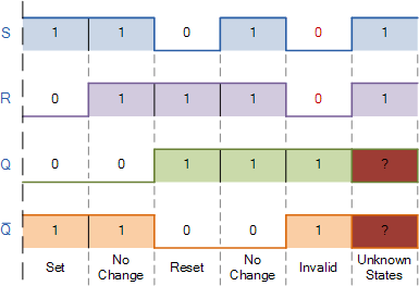
This unbalance can cause one of the outputs to switch faster than the other resulting in the flip-flop switching to one state or the other which may not be the required state and data corruption will exist. This unstable condition is generally known as its Meta-stable state.
Then, a bistable SR flip-flop or SR latch is activated or set by a logic “1” applied to its S input and deactivated or reset by a logic “1” applied to its R. The SR flip-flop is said to be in an “invalid” condition (Meta-stable) if both the set and reset inputs are activated simultaneously.
As well as using NAND gates, it is also possible to construct simple one-bit SR Flip-flops using two cross-coupled NOR gates connected in the same configuration. The circuit will work in a similar way to the NAND gate circuit above, except that the inputs are active HIGH and the invalid condition exists when both its inputs are at logic level “1”, and this is shown below.
The NOR Gate SR Flip-flop
Switch Debounce Circuits
Edge-triggered flip-flops require a nice clean signal transition, and one practical use of this type of set-reset circuit is as a latch used to help eliminate mechanical switch “bounce”. As its name implies, switch bounce occurs when the contacts of any mechanically operated switch, push-button or keypad are operated and the internal switch contacts do not fully close cleanly, but bounce together first before closing (or opening) when the switch is pressed.
This gives rise to a series of individual pulses which can be as long as tens of milliseconds that an electronic system or circuit such as a digital counter may see as a series of logic pulses instead of one long single pulse and behave incorrectly. For example, during this bounce period the output voltage can fluctuate wildly and may register multiple input counts instead of one single count. Then set-reset SR Flip-flops or Bistable Latch circuits can be used to eliminate this kind of problem and this is demonstrated below.
SR Flip Flop Switch Debounce Circuit
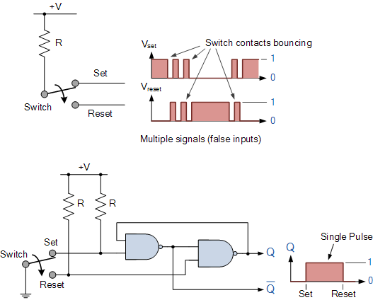
Depending upon the current state of the output, if the set or reset buttons are depressed the output will change over in the manner described above and any additional unwanted inputs (bounces) from the mechanical action of the switch will have no effect on the output at Q.
When the other button is pressed, the very first contact will cause the latch to change state, but any additional mechanical switch bounces will also have no effect. The SR flip-flop can then be RESET automatically after a short period of time, for example 0.5 seconds, so as to register any additional and intentional repeat inputs from the same switch contacts, such as multiple inputs from a keyboards “RETURN” key.
Commonly available IC’s specifically made to overcome the problem of switch bounce are the MAX6816, single input, MAX6817, dual input and the MAX6818 octal input switch debouncer IC’s. These chips contain the necessary flip-flop circuitry to provide clean interfacing of mechanical switches to digital systems.
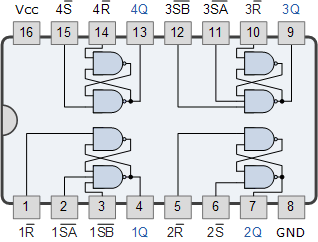
Set-Reset bistable latches can also be used as Monostable (one-shot) pulse generators to generate a single output pulse, either high or low, of some specified width or time period for timing or control purposes. The 74LS279 is a Quad SR Bistable Latch IC, which contains four individual NAND type bistable’s within a single chip enabling switch debounce or monostable/astable clock circuits to be easily constructed.
Quad SR Bistable Latch 74LS279
Gated or Clocked SR Flip-Flop
It is sometimes desirable in sequential logic circuits to have a bistable SR flip-flop that only changes state when certain conditions are met regardless of the condition of either the Set or the Reset inputs. By connecting a 2-input AND gate in series with each input terminal of the SR Flip-flop a Gated SR Flip-flop can be created. This extra conditional input is called an “Enable” input and is given the prefix of “EN“. The addition of this input means that the output at Q only changes state when it is HIGH and can therefore be used as a clock (CLK) input making it level-sensitive as shown below.
Gated SR Flip-flop
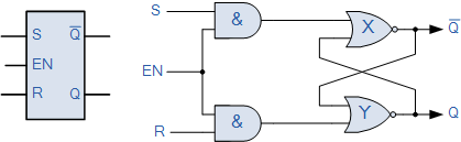
When the Enable input “EN” is at logic level “0”, the outputs of the two AND gates are also at logic level “0”, (AND Gate principles) regardless of the condition of the two inputs S and R, latching the two outputs Q and Q into their last known state. When the enable input “EN” changes to logic level “1” the circuit responds as a normal SR bistable flip-flop with the two AND gates becoming transparent to the Set and Reset signals. This additional enable input can also be connected to a clock timing signal (CLK) adding clock synchronisation to the flip-flop creating what is sometimes called a “Clocked SR Flip-flop“. So a Gated Bistable SR Flip-flop operates as a standard bistable latch but the outputs are only activated when a logic “1” is applied to its EN input and deactivated by a logic “0”. In the next tutorial about Sequential Logic Circuits, we will look at another type of simple edge-triggered flip-flop which is very similar to the RS flip-flop called a JK Flip-flop named after its inventor, Jack Kilby. The JK flip-flop is the most widely used of all the flip-flop designs as it is considered to be a universal device.