Theoretical Paper
- Computer Organization
- Data Structure
- Digital Electronics
- Object Oriented Programming
- Discrete Mathematics
- Graph Theory
- Operating Systems
- Software Engineering
- Computer Graphics
- Database Management System
- Operation Research
- Computer Networking
- Image Processing
- Internet Technologies
- Micro Processor
- E-Commerce & ERP
Practical Paper
Industrial Training

Half Adder and Full Adder Circuit
Half Adder and Full Adder circuits is explained with their truth tables in this article. Design of Full Adder using Half Adder circuit is also shown.Single-bit Full Adder circuit and Multi-bit addition using Full Adder is also shown.
TAKE A LOOK : BOOLEAN LOGIC
TAKE A LOOK : LOGIC GATES
TAKE A LOOK : FLIP FLOPS
Half Adder
With the help of half adder, we can design circuits that are capable of performing simple addition with the help of logic gates.
Let us first take a look at the addition of single bits.
0+0 = 0
0+1 = 1
1+0 = 1
1+1 = 10
These are the least possible single-bit combinations. But the result for 1+1 is 10. Though this problem can be solved with the help of an EXOR Gate, if you do care about the output, the sum result must be re-written as a 2-bit output.
Thus the above equations can be written as
0+0 = 00
0+1 = 01
1+0 = 01
1+1 = 10
Here the output ‘1’of ‘10’ becomes the carry-out. The result is shown in a truth-table below. ‘SUM’ is the normal output and ‘CARRY’ is the carry-out.
INPUTS OUTPUTS
| A | B | SUM | CARRY |
| 0 | 0 | 0 | 0 |
| 0 | 1 | 1 | 0 |
| 1 | 0 | 1 | 0 |
| 1 | 1 | 0 | 1 |
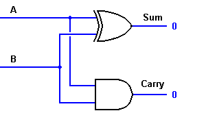
From the equation it is clear that this 1-bit adder can be easily implemented with the help of EXOR Gate for the output ‘SUM’ and an AND Gate for the carry. Take a look at the implementation below.
For complex addition, there may be cases when you have to add two 8-bit bytes together. This can be done only with the help of full-adder logic.
Full Adder
This type of adder is a little more difficult to implement than a half-adder. The main difference between a half-adder and a full-adder is that the full-adder has three inputs and two outputs. The first two inputs are A and B and the third input is an input carry designated as CIN. When a full adder logic is designed we will be able to string eight of them together to create a byte-wide adder and cascade the carry bit from one adder to the next.
The output carry is designated as COUT and the normal output is designated as S. Take a look at the truth-table.
INPUTS OUTPUTS
| A | B | CIN | COUT | S |
| 0 | 0 | 0 | 0 | 0 |
| 0 | 0 | 1 | 0 | 1 |
| 0 | 1 | 0 | 0 | 1 |
| 0 | 1 | 1 | 1 | 0 |
| 1 | 0 | 0 | 0 | 1 |
| 1 | 0 | 1 | 1 | 0 |
| 1 | 1 | 0 | 1 | 0 |
| 1 | 1 | 1 | 1 | 1 |
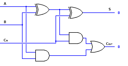
From the above truth-table, the full adder logic can be implemented. We can see that the output S is an EXOR between the input A and the half-adder SUM output with B and CIN inputs. We must also note that the COUT will only be true if any of the two inputs out of the three are HIGH.
Thus, we can implement a full adder circuit with the help of two half adder circuits. The first will half adder will be used to add A and B to produce a partial Sum. The second half adder logic can be used to add CIN to the Sum produced by the first half adder to get the final S output. If any of the half adder logic produces a carry, there will be an output carry. Thus, COUT will be an OR function of the half-adder Carry outputs. Take a look at the implementation of the full adder circuit shown below.
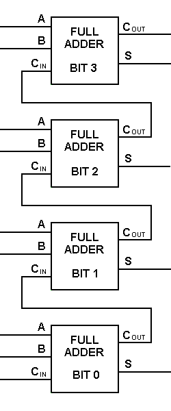
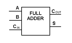
Though the implementation of larger logic diagrams is possible with the above full adder logic a simpler symbol is mostly used to represent the operation. Given below is a simpler schematic representation of a one-bit full adder.
With this type of symbol, we can add two bits together taking a carry from the next lower order of magnitude, and sending a carry to the next higher order of magnitude. In a computer, for a multi-bit operation, each bit must be represented by a full adder and must be added simultaneously. Thus, to add two 8-bit numbers, you will need 8 full adders which can be formed by cascading two of the 4-bit blocks. The addition of two 4-bit numbers is shown below.