Theoretical Paper
- Computer Organization
- Data Structure
- Digital Electronics
- Object Oriented Programming
- Discrete Mathematics
- Graph Theory
- Operating Systems
- Software Engineering
- Computer Graphics
- Database Management System
- Operation Research
- Computer Networking
- Image Processing
- Internet Technologies
- Micro Processor
- E-Commerce & ERP
Practical Paper
Industrial Training

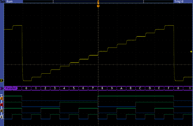
R-2R Ladder circuit
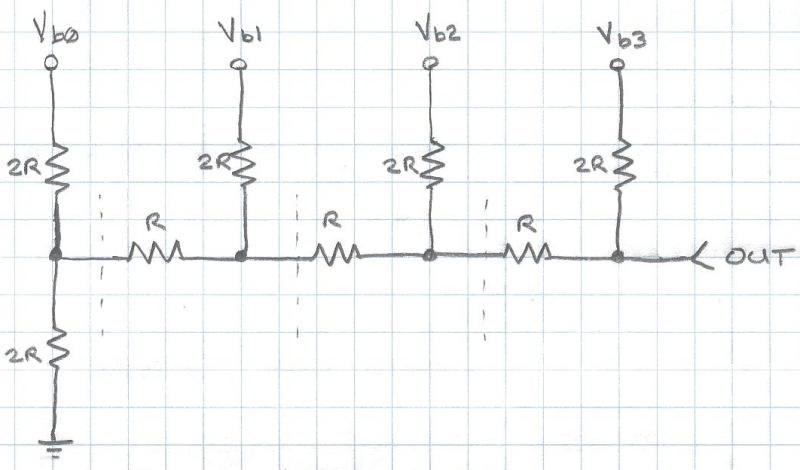
With the recent announcement of the world’s fastest Digital to Analog Converter (DAC) from Tektronix Component Solutions, I thought it would be interesting to take a quick tutorial tour through one of the simplest DAC architectures – the R-2R resistor ladder network as shown in Figure 1below.
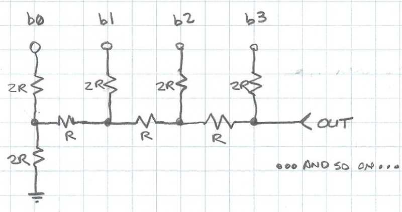
The R-2R resistor ladder network directly converts a parallel digital symbol/word into an analog voltage. Each digital input (b0, b1, etc.) adds its own weighted contribution to the analog output. This network has some unique and interesting properties.
Easily scalable to any desired number of bits
Uses only two values of resistors which make for easy and accurate fabrication and integration
Output impedance is equal to R, regardless of the number of bits, simplifying filtering and further analog signal processing circuit design
Analyzing the R-2R network brings back memories of the seemingly infinite variety of networks that you’re asked to solve during your undergraduate electrical engineering studies. The reality though, is that the analysis of this network and how it works is quite simple. By methodical application of Thevenin Equivalent circuits and Superposition, we can easily show how the R-2R circuit works.
Let’s start off by analyzing the output impedance. Working through the circuit, simplifying it with Thevenin equivalents, makes this process simple. Thevenin says that if your circuit contains linear elements like voltage sources, current sources and resistors, that you can cut your circuit at any point and replace everything on one side of the cut with a voltage source and a single series resistor. The voltage source is the open-circuit voltage at the cut point, and the series resistor is the equivalent open circuit resistance with all voltage sources shorted.
Figure 2 below shows the locations of the “cut lines” we’ll use to simplify this circuit to calculate its output impedance. For this analysis, the digital inputs will all be considered shorted to ground.
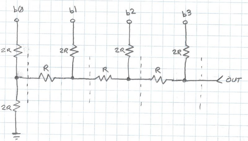
The two 2R resistors to the left of the first cut line in Figure 2 appear in parallel (when the digital bit b0 is grounded), and can be replaced with a single resistor R as shown in Figure 3. The series combination of the two R resistors on the left of Figure 3 combine to a single resistor of value 2R, which is in parallel with the 2R resistor to b1.
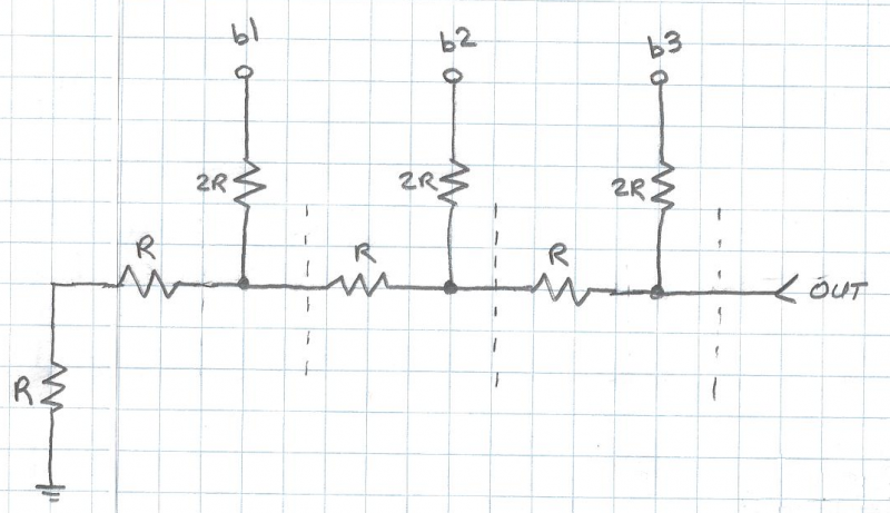
You may notice that this process repeats itself each time we work from left to right, successively replacing combinations of resistors with their equivalents. As you can see in Figure 4, the circuit ultimately simplifies to a single resistor R.
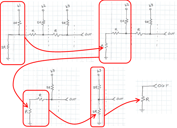
Thus, the output impedance of the R-2R resistor network is always equal to R, regardless of the size (number of bits) of the network. This simplifies the design of any filtering, amplification or additional analog signal conditioning circuitry that may follow the network.
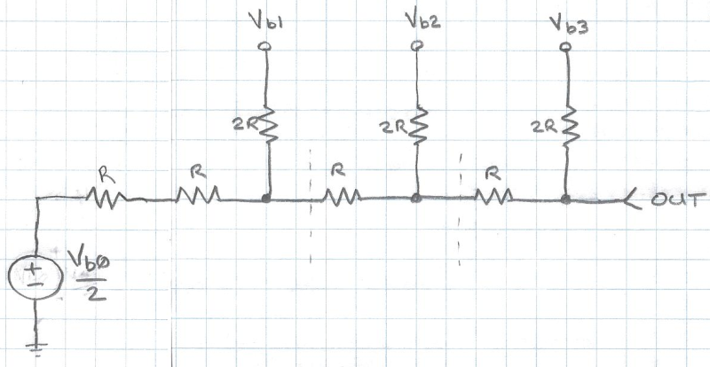
Next, we’ll look at how to calculate the analog voltage output for a given parallel digital input on the b0, b1, etc. inputs. We’ll use the same Thevenin equivalents technique shown above, as well as Superposition. Superposition tells us that if you individually compute the contribution of a given source to the output (with all others voltage sources shorted and current sources opened), you can then sum the results for each of the sources to obtain the final result for the output.
We’ll calculate the contribution of two of the bits of our 4-bit R-2R DAC in Figure 5 to show the process. We’ll assume the bits b0 and b2 are logic high, and bits b1 and b3 are logic low (ground).
We start by replacing the circuit to the left of the left-most cut-line with its Thevenin equivalent. Figure 6 shows the Thevenin equivalent, which is the series resistor of value R (parallel combination of two 2R resistors), and the open circuit voltage from the resistor divider (Vb0/2).
The process continues methodically, step by step for each cut-line, substituting the equivalent circuit for each stage, as shown graphically in Figure 7.
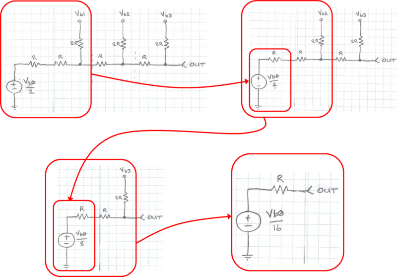
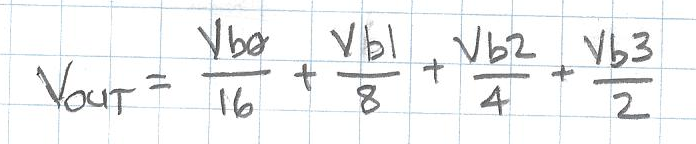
We can see that the voltage contribution from bit b0 is 1/16th of the logic high voltage level. Each bit stage that this voltage passes through cuts the contribution by a factor of 2. You may begin to see a theme here…
Next, we’ll compute the contribution from bit b2, as shown in Figure 8 below:
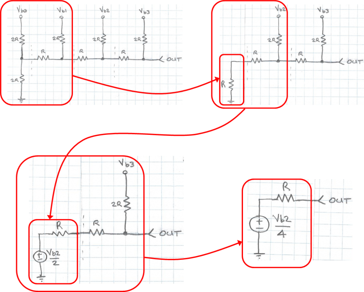
From the Thevenin equivalent analysis shown earlier, we know that we can replace any portion of this circuit to the left of any of the cut lines with a resistor of value R, shown as the first step in Figure 8. Next, we follow the same Thevenin equivalent process to the output. As you may have already suspected, the contribution of bit b2 is simply Vb2/4. Thus, the analog output voltage when bits b0 and b2 are equal to logic one is simply given by Vb0/16 + Vb2/4.
In a more general sense, the contribution of each bit to the output is a simple binary weighting function of each bit. As you work back from the MSB to the LSB, the voltage contribution each bit is cut in half. Thus, the general form of the equation to calculate the output voltage is shown in Figure
The R-2R resistor ladder based digital-to-analog converter (DAC) is a simple, effective, accurate and inexpensive way to create analog voltages from digital values. Monolithic R-2R resistor networks are available from various resistor component manufacturers, making it easy to incorporate them into your designs.