Theoretical Paper
- Computer Organization
- Data Structure
- Digital Electronics
- Object Oriented Programming
- Discrete Mathematics
- Graph Theory
- Operating Systems
- Software Engineering
- Computer Graphics
- Database Management System
- Operation Research
- Computer Networking
- Image Processing
- Internet Technologies
- Micro Processor
- E-Commerce & ERP
Practical Paper
Industrial Training

E2PROM Interfacing With A PC
E2PROM Interfacing With A PC
E2PROM expands to Electronically Erasable Programmable Read-only Memory. This is in the form of an IC ( Integrated Circuits ) or SMDs ( Surface Mount Devices ) whichever the variant the main purpose of it is to store data without power backup. That is, once data is written on it, it will remain written independent of any power supply. This is important in today’s world where identities are becoming more and more digital. People, Machines, Goods, need to be identified independent of one another and also independent of any human intervention. These devices are small and cheep, and can be used in almost any kind of environment. We are already living in a world full of these tiny gizmos.
An E2PROM is guaranteed to work for about 10000 read / write operations. It also promises to store data for at least a decade and in some cases up to 4 decades. In this article we will not be looking at how an E2PROM actually stores data or how it keeps it true for such a long time without batteries. What we are interested in here is how best we can use a home PC to take full advantage of this wonder chip.
Our test E2PROM is a small IC with 1024 bits (128 bytes) of EE memory. It works with a normal 5V DC supply and is simple to interface with a PC. For Electronics buffs the IC we are using is NM93C46 serial E2PROM. Our program will write an integer ( 16-bit value ) at a predetermined location in the memory and retrieve it. This IC has 64 registers each of size 16-bits. The IC will be interfaced with the LPT port of a PC. The circuit for the same is shown in Figure 1.
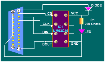
Figure 1.
For our example we have not provided any separate power supply, instead we are using the Strobe pin (Pin 1) of the LPT as our power source. Ground for the source is the common ground on the LPT (Pins 18 – 25).
A few things about the E2PROM IC now: The IC has 8 pins, we will be using 6 of them. Pin number 6 and 7 will be left open. The functions of each pins are:
Pin 1: Clock Select.
Pin 2: Clock
Pin 3: Data In
Pin 4: Data Out.
Pin 5: Power Input
Pin 8: Ground.
In the circuit we have connected a diode in between strobe of the LPT and the power source pin of the IC. This arrangement is made to protect the IC from accidental reverse voltage and consequently reverse current. Reverse current will damage the IC in an unpredictable manner. A diode allows current to flow in one direction only and acts as an insulator for the reverse direction. This makes it ideal for this job. The other place where we have connected the diode is between the power pin and the ground pin. This arrangement also works as a safety mechanism to limit the amount of current flowing through the IC. Our first diode will not allow reverse current but it is helpless when excess current flows in. To protect our IC against this the power pin is connected to the ground pin via the 220-Ohm resistance. And the ground is connected to the ground of the LPT. Any excess current flowing into the circuit will be passed on through the resistance to ground, bypassing the IC.
Here is what each pin of the IC is intended to do:
Sending logic 1 ( +5 V signal ) to the Chip Select will tell the IC that it needs to be ready to perform some action. Logic 1 on the Clock will cause the chip to read / write data from / to the Data In / Data Out pins of the IC. Jobs of Data In and Data Out pins are self-explanatory.
On the LPT port side, we are interested in two of its ports the Data Port and the Status Port. The Data Port is being used to send signals and the Status Port is receiving information. We use pin number 13 of the LPT port connector. This is the pin on the status port, we use this to get data from the IC. Pins 2, 3, 4 are connected to Chip-Select, Clock and Data-In pins of the E2PROM IC respectively. Pin 1 on the LPT connector serves as the power source and is connected to the power pin of the E2PROM IC. All grounds are shorted.
Getting down to the programming part of this article, here is the source code:
#include <stdio.h>
#include <conio.h>
#define PORTA 0x378 /* Address of LPT */
#define PORTB 0x379
#define CS 0x01 /* Chip Select */
#define STARTBIT 0x01
/* our address value can be changed */
#define DATA_ADD1 0x00
void write_bit ( unsigned int data )
{
if ( data == 0 )
{
data = ( CS ) ;
outportb ( PORTA, data ) ;
}
else
{
data = ( CS | 0x02 ) ; /*mask all bits except data */
outportb ( PORTA, data ) ;
}
data = ( data | 0x04 ) ;
outportb ( PORTA, data ) ; /* Give Clock Pulse */
data = ( data ^ 0x04 ) ;
outportb ( PORTA, data ) ; /* Remove Clock Pulse */
data = ( CS ) ;
outportb ( PORTA, data ) ;
return;
}
unsigned int read_bit( )
{
unsigned int data, rv ;
data = ( CS | 0x04 ) ;
outportb ( PORTA, data ) ; /* Apply Clock Pulse */
rv = inportb ( PORTB ) ; /* Read Data From Input port */
data = ( data ^ 0x04 ) ;
outportb ( PORTA, data ) ; /* Remove Clock Pulse */
rv = rv & 0x10 ; /* Mask Everything Except Data */
if ( rv == 0 )
data = 0x0 ;
else
data = 0x01 ;
return data ;
}
void enable_9346( )
{
outportb ( PORTA, CS ) ;
write_bit ( STARTBIT ) ;
write_bit ( 0x00 ) ;
write_bit ( 0x00 ) ;
write_bit ( 0x01 ) ;
write_bit ( 0x01 ) ;
write_bit ( 0x00 ) ;
write_bit ( 0x00 ) ;
write_bit ( 0x00 ) ;
write_bit ( 0x00 ) ;
outportb ( PORTA, 0x00 ) ;
}
void disable_9346( )
{
outportb ( PORTA, CS ) ;
write_bit ( STARTBIT ) ;
write_bit ( 0x00 ) ;
write_bit ( 0x00 ) ;
write_bit ( 0x00 ) ;
write_bit ( 0x00 ) ;
write_bit ( 0x00 ) ;
write_bit ( 0x00 ) ;
write_bit ( 0x00 ) ;
write_bit ( 0x00 ) ;
outportb ( PORTA, 0x00 ) ;
}
void write_9346 ( int my_add, unsigned int my_data )
{
unsigned int i, new_add, new_data ;
unsigned long int j ;
outportb ( PORTA, CS ); /* Give Chip Select High To Write A Bit */
write_bit ( STARTBIT ) ; /* Give Start Bit TO Write A Bit */
write_bit ( 0x00 ) ; /* Give Mode Bit 1 For Writing Operation */
write_bit ( 0x01 ) ; /* Give Mode Bit 2 For Writing Operation */
j = 0x20 ;
for ( i = 0 ; i < 6 ; i++ )
{
new_add = my_add & j ;
write_bit ( new_add ) ;
j = j >> 1 ;
}
j = 0x8000 ; /* j Is A 16 Bit Masking Number */
for ( i = 0 ; i < 16 ; i++ )
{
new_data = my_data & j ; /* Mask All Except Current Bit */
write_bit ( new_data ) ;
j = j >> 1 ;
}
outportb ( PORTA, 0x00 ) ; /* Remove Chip Select */
}
unsigned int read_9346 ( int my_add )
{
unsigned int i, j, new_add, my_bit ;
unsigned long int my_data ;
outportb ( PORTA, CS ) ; /* Set Chip Select ON */
write_bit ( STARTBIT ) ; /* Give A Start Bit to read Data */
write_bit ( 0x01 ) ; /* Give Mode Bit 1 For Read Operation */
write_bit ( 0x00 ) ; /* Give Mode Bit 2 For Read Operation */
j = 0x20 ;
for ( i = 0 ; i < 6 ; i++ )
{
new_add = my_add & j ;
write_bit ( new_add ) ;
j = j >> 1 ;
}
my_data = 0x0000 ;
for ( i = 0 ; i < 16 ; i++ )
{
my_data = my_data << 1 ;
my_bit = read_bit( ) ; /* GetOne Bit Of Data */
my_data = my_bit | my_data ; /* Setup Read Bit Into Data */
}
outportb ( PORTA, 0x00 ) ; /* Remove Port Select */
return my_data ;
}
void main( )
{
unsigned int data, info ;
clrscr( ) ;
enable_9346( ) ;
delay ( 10 ) ;
printf ( "Enter value to be stored in the chip: " ) ;
scanf ( "%d", &data ) ;
/* writing begins here */
enable_9346( ) ;
delay ( 10 ) ;
write_9346 ( DATA_ADD1, data ) ;
delay ( 10 ) ;
disable_9346( ) ;
printf ( "Press any key to read back the data...\n" ) ;
getch( ) ;
/* reading begins here */
enable_9346( ) ;
delay ( 10 ) ;
info = read_9346 ( DATA_ADD1 ) ;
printf ( "Value read from chip is: %d\n", info ) ;
disable_9346( ) ;
getch( ) ;
}
The program is basically divided into three parts, reading a number from the user, writing it on the IC, and finally reading it and displaying it.
This procedure sounds simple but it is not. It must be clear from the program that lot many things have to be done to achieve this simple task of reading and writing things from and to the E2PROM.
We have declared 6 functions in this program, each with a specific job.
| write_bit( ) | It will writes one bit of data at a pre decided address. |
| read_bit( ) | This reads one bit from the IC again from a pre set address. |
| write_9346( ) | Will use the above declared functions to first communicate the address and write data there. |
| read_9346( ) | Reads first it will communicate the address and then read data serially from the IC. |
| enable_9346( ) | This instruction will enable the chip for further communication. |
| disable_9346( ) | After the communication with the IC is over, always use this function to disable it. |
Enable and disable functions work in tandem with each other, there is a complex protocol dictated by the chip architecture for this. We as users don’t have a choice to alter that protocol.
Lets have a look at the things that we can alter.
The write_bit( ) function is fairly generic and can be used for almost any bit wise writing operation. This function writes one bit of data on the Data-In Pin of the E2PROM IC. the second bit on the 378h port of the LPT needs to be set accordingly.
read_bit( ) function will read data from the Data-Out pin of the E2PROM IC. There is though a prerequisite to this, the user needs to initiate the mode of working of the IC to reading before doing this. By default the IC is in no activity mode on this pin. Unlike in the case of write_bit( ) where we can always write on the Chip-Select pin without worrying about the mode in which the IC is.
write_9346( ) writes full 16 bits of information on the IC the procedure simple, first select the bit by giving it a true logic ( +5 V ) signal in the Chip-Select pin of the IC, followed by giving the start bit to ask the IC to listen to data sent next. The following two bits are the mode select bits. Mode select tells the IC whether to read from or right to the 6-bit address following it. Once this is done, send the 6-bit address and finally the 16-bit value to be written.
read_9346( ) works similar to the write_9346( ) function. Except for the mode and call to read_bit( ) almost nothing has changed. Each bit wise value received will be inserted into the integer data variable at proper location.
The reason why we are passing a 6 bit address and a 16 bit data value is that we have only 64 memory locations each of size 16 bits. 64 registers can be separately addressed using 6 bits.
The delay( 10 ) calls in our program are essential as the chip takes approximately 3.5 milliseconds to process instructions that we pass on to it. The 10 millisecond margin that we use here is just a precaution we take to be on the safer side.
And again as usual this program might not work on Windows NT family of operating systems. I strongly believe that if we can read and write one bit of information from only one address, extending the logic for multiple bits and multiple addresses id just a matter of sparing some time.