Theoretical Paper
- Computer Organization
- Data Structure
- Digital Electronics
- Object Oriented Programming
- Discrete Mathematics
- Graph Theory
- Operating Systems
- Software Engineering
- Computer Graphics
- Database Management System
- Operation Research
- Computer Networking
- Image Processing
- Internet Technologies
- Micro Processor
- E-Commerce & ERP
Practical Paper
Industrial Training

Timing Diagrams
It is one of the best way to understand to process of micro-processor/controller. With the help of timing diagram we can understand the working of any system, step by step working of each instruction and its execution, etc.
It is the graphical representation of process in steps with respect to time. The timing diagram represents the clock cycle and duration, delay, content of address bus and data bus, type of operation ie. Read/write/status signals.
Important terms related to timing diagrams:
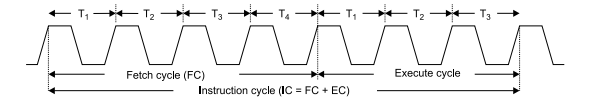
- 1. Instruction cycle: this term is defined as the number of steps required by the cpu to complete the entire process ie. Fetching and execution of one instruction. The fetch and execute cycles are carried out in synchronization with the clock.
- 2. Machine cycle: It is the time required by the microprocessor to complete the operation of accessing the memory devices or I/O devices. In machine cycle various operations like opcode fetch, memory read, memory write, I/O read, I/O write are performed.
- 3. T-state: Each clock cycle is called as T-states.
Rules to identify number of machine cycles in an instruction:
1. If an addressing mode is direct, immediate or implicit then No. of machine cycles = No. of bytes.
2. If the addressing mode is indirect then No. of machine cycles = No. of bytes + 1. Add +1 to the No. of machine cycles if it is memory read/write operation.
3. If the operand is 8-bit or 16-bit address then, No. of machine cycles = No. of bytes +1.
4. These rules are applicable to 80% of the instructions of 8085.
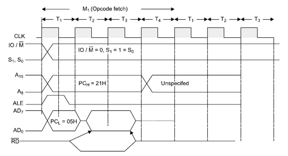
Timing Diagram:
Opcode fetch:
The microprocessor requires instructions to perform any particular action. In order to perform these actions microprocessor utilizes Opcode which is a part of an instruction which provides detail(ie. Which operation µp needs to perform) to microprocessor.
Operation:
Read and write timing diagram for memory and I/O Operation
Memory Read: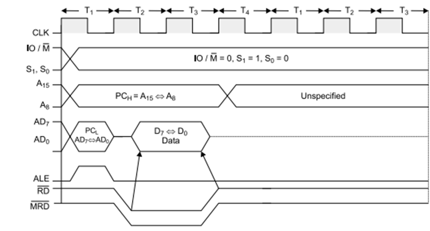
Figure: Memory read timing diagram
Operation:
Memory Write:
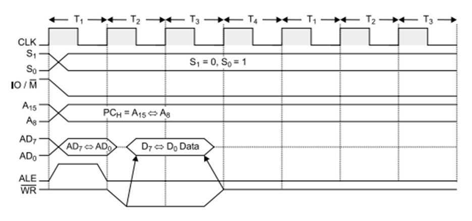
Figure: Memory write timing diagram
Operation:
IO Read:
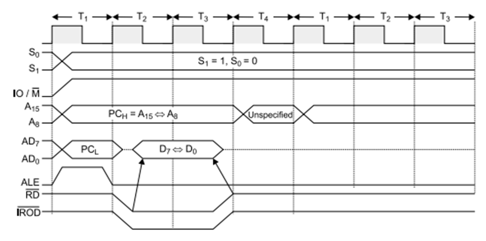
Operation:
It is used to fetch one byte from an IO port.
It requires 3 T-States.
During T1, The Lower Byte of IO address is duplicated into higher order address bus A8-A15.
ALE is high and AD0-AD7 contains address of IO device.
IO/M (bar) goes high as it is an IO operation.
During T2, ALE goes low, RD (bar) goes low and data appears on AD0-AD7 as input from IO device.
During T3 Data remains on AD0-AD7 till RD(bar) is low.
IO Write:
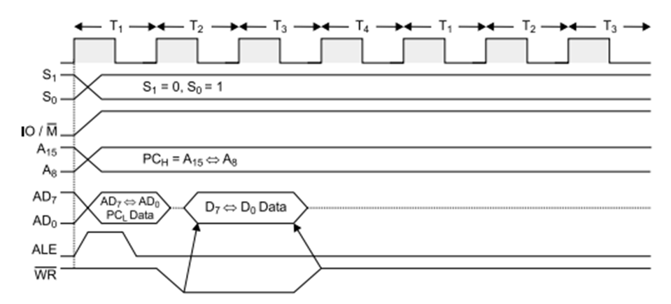
Operation: