Theoretical Paper
- Computer Organization
- Data Structure
- Digital Electronics
- Object Oriented Programming
- Discrete Mathematics
- Graph Theory
- Operating Systems
- Software Engineering
- Computer Graphics
- Database Management System
- Operation Research
- Computer Networking
- Image Processing
- Internet Technologies
- Micro Processor
- E-Commerce & ERP
Practical Paper
Industrial Training

Display Interfacing
In a microprocessor b system, when keyboard and 7-segment LED display is interfaced using ports or latches then the processor has to carry the following task.
Keyboard scanning
Key debouncing
Key code generation
Sending display code to LED
Display refreshing
Interfacing 8279 with 8085 processor:
A typical Hexa keyboard and 7-segment LED display interfacing circuit using 8279 is shown.
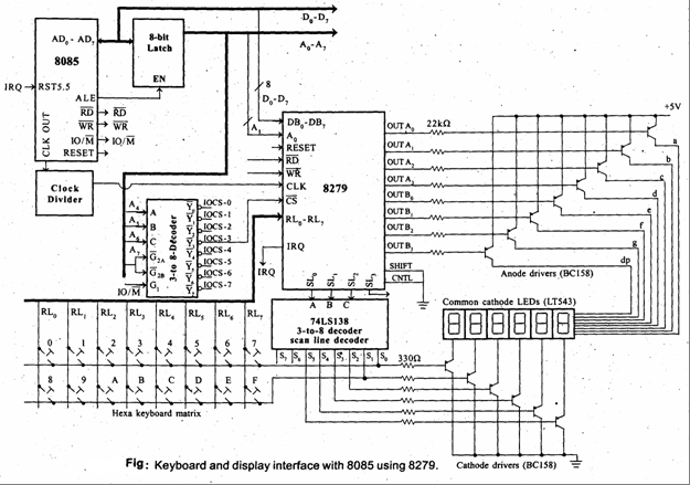
The circuit can be used in 8085 microprocessor system and consist of 16 numbers of hexa-keys and 6 numbers of 7-segment LEDs.
The 7-segment LEDs can be used to display six digit alphanumeric character.
The 8279 can be either memory mapped or I/O mapped in the system. In the circuit shown is the 8279 is I/O mapped.
The address line A0 of the system is used as A0 of 8279.
The clock signal for 8279 is obtained by dividing the output clock signal of 8085 by a clock divider circuit.
The chip select signal is obtained from the I/O address decoder of the 8085 system. The chip select signals for I/O mapped devices are generated by using a 3-to-8 decoder.
The address lines A4, A5 and A6 are used as input to decoder.
The address line A7 and the control signal IO/M (low) are used as enable for decoder.
The chip select signal IOCS-3 is used to select 8279.
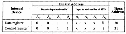
The I/O address of the internal devices of 8279 are shown in table.
The circuit has 6 numbers of 7-segment LEDs and so the 8279 has to be programmed in encoded scan. (Because in decoded scan, only 4 numbers of 7-segment LEDs can be interfaced)
In encoded scan the output of scan lines will be binary count. Therefore an external, 3-to-8 decoder is used to decode the scan lines SL0, SL1 and SL2 of 8279 to produce eight scan lines S0 to S7.
The decoded scan lines S0 and S1 are common for keyboard and display.
The decoded scan lines S2 to S5 are used only for display and the decoded scan lines S6 and S7 are not used in the system.
Anode and Cathode drivers are provided to take care of the current requirement of LEDs.
The pnp transistors, BC 158 are used as driver transistors.
The anode drivers are called segment drivers and cathode drivers are called digit drivers.
The 8279 output the display code for one digit through its output lines (OUT A0 to OUT A3 and OUT B0 to OUT B3) and send a scan code through, SL0- SL3.
The display code is inverted by segment drivers and sent to segment bus.
The scan code is decoded by the decoder and turns ON the corresponding digit driver. Now one digit of the display character is displayed. After a small interval (10 milli-second, typical), the display is turned OFF (i.e., display is blanked) and the above process is repeated for next digit. Thus multiplexed display is performed by 8279.
The keyboard matrix is- formed using the return lines, RL0 to RL3 of 8279 as columns and decoded scan lines S0 and S1 as rows.
A hexa key is placed at the crossing point of each row and column. A key press will short the row and column. Normally the column and row line will be high.
During scanning the 8279 will output binary count on SL0 to SL3, which is decoded by decoder to make a row as zero. When a row is zero the 8279 reads the columns. If there is a key press then the corresponding column will be zero.
If 8279 detects a key press then it wait for debounce time and again read the columns to generate key code.
In encoded scan keyboard mode, the 8279 stores an 8-bit code for each valid key press. The keycode consist of the binary value of the column and row in which the key is found and the status of shift and control key.
After a scan time, the next row is made zero and the above process is repeated and so on. Thus 8279 continuously scan the keyboard.